
Tech Talk
Embedded Systems Prototyping
By Doug Bell | Principal Engineer

Modern audio electronics technologies involve immense complexities. They fill a spectrum from simple integrated circuits to full microprocessor systems with operating systems like Linux. The capabilities of modern chips come with the responsibility of the user to properly configure and operate them – they are not passive devices. Even rather simple integrated circuits require basic configuration just to establish default operation. This is done by providing proper voltages at various pins on the chip – often 0 or 3.3V for digital devices. Further configuration is done by setting values in their internal memory locations known as registers. There can be dozens (even hundreds!) of registers. Such devices are “programmable” in the sense that an engineer must provide the desired parameters beyond default values. In more complex devices like video receivers there is occasionally “microcode” – internal programming running on the chip - which is inaccessible to the user of the chip.
In a system, this programming is done by a “host” microcontroller which would run a program to dispatch proper values to the other chips in the system at initialization. Much of the complexity in writing software for a system is in this initial configuration – doing operations correctly and in the right order to attain a valid initial state. During subsequent operation such a host program would, for example, detect an encoder rotation and adjust volume at volume control circuitry by sending updated information. Software engineers’ responsibilities include writing such programs which interface with function-specific hardware.
So say you have a product concept and some chips which should do the job – what next? Anyone unfamiliar with electronics might have some vague concept that you design some circuit boards with some chips, get some boards made, maybe fix some stuff, and YOU’RE DONE. This would generally be expensive, immensely error prone, excessively time consuming, and incomplete. Further, there is significant work in software to breathe life into systems.
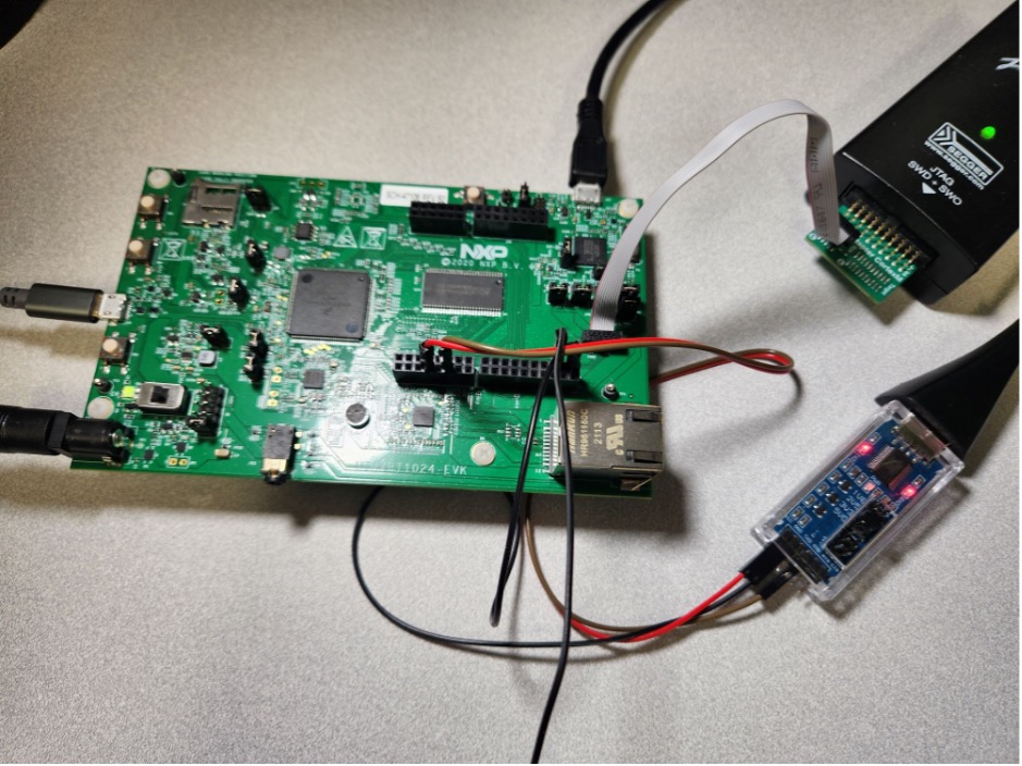
Engineers often develop systems using “development kits” (AKA “Dev Boards” or “Reference Boards”) which are typically circuit boards available from a chip manufacturer designed to facilitate quick startup. They’re often fairly inexpensive and very versatile, showcasing the chip’s capabilities. The schematic and layout of this board is typically made available for easy adaptation to the engineers’ final design. Sometimes specific layout techniques or peripheral components are critical – hence the utility of a reference hardware design. Chip manufacturers are interested in getting a workable design with their chips done, and getting chips sold, so anything they can do to facilitate that is in the interest of everyone.
Dev boards often have “jumpers” – wiring access points to let the user connect or disconnect wiring in the circuitry to configure the system. Additionally, there can be various connectors for input and output signals, buttons, switches, LEDs, displays, etc. “Headers” are wiring ports with multiple signals.
Configuring and using the dev board is where the fun starts. Hopefully the documentation is clear, explicit, complete, and correct but this isn’t always the case, especially on less mature and/or less mainstream products. One may consider the country of origin as well – translation issues occur. Not out of the question are anomalies with the board – ambiguities about behavior, actual hardware design errors, issues between revisions of the dev board, parts failing, etc. Even with perfect documentation and hardware, it can be quite challenging going from what you want to happen to what needs to happen at the chip level. Sometimes one must “read between the lines” to understand from a datasheet how to set up a chip for a certain outcome.
Beyond configuration possible via jumpers, DIP switches, etc., it commonly becomes a software engineer’s responsibility to further configure and operate these boards to achieve the desired functionality. This is done with an external PC.
There is often some serial data connection to send information between the PC and the dev board. In more basic situations the PC would run “Teraterm” (on Windows) or a similar standard terminal program to talk to the dev board. Commands issued would configure the dev board and indicate operational status. More complex boards may come with a vendor-supplied utility with a GUI interface to accomplish this configuration and status reporting. The connection could be USB, standard RS-232, or a 3.3V or 5V level UART signal at the dev board run through an adapter to have USB for the PC side.
A dev board for a DAC might have rudimentary capabilities using “hardware mode” where various features or configurations are set by jumpers, DIP switches, etc. Alternatively, “software mode” allows full access on the fly to all chip capabilities via programming. A typical feature of chips such as a DAC is an array of registers – memory locations- each of which serve a particular control ( and/or indication ) function. These are commonly accessed via an I2C bus. A host microcontroller in the system can read and write these registers. Many registers have obscure functionality and are left at a default state from power up. In a real system a program might regularly monitor some registers to detect changes in order to act accordingly. For example, a sample rate change could be detected for display on a front panel.
Development kits exist for microcontrollers as well. In this case a connection to a PC lets an engineer write code on her PC, download it to the dev board, and debug it. This is done on the PC using an Integrated Development Environment (or IDE) which allows editing, compiling, and debugging of code. The IDE facilitates various debugging techniques including “breakpoints” (stopping code at various places), checking or modifying memory contents, and printing out human readable messages. Once code is deemed workable it can run independently of the host PC and any debugger.
Say you want to create a prototype system using a few different new chips – each with their own dev board. Since they each work on their own, one would just connect them together and be done, right? Not even close.
To start, what’s a sensible layout to put them in? Once you arrange them all on a common platform or chassis you’ll probably need to access something on the underside of a board. You may run into issues with grounding, signal degradation between boards, power sequencing and reset timing problems, plain old loose wire problems, and power tree considerations (who powers what and when).
Such prototyping efforts are far from a workable product design but does allow checking of critical features, listening tests, technology proof of concept, chip comparisons, changing of settings, etc. Some less tangible benefits of showing a prototype include identifying “gotchas” and getting momentum on a project. All these are invaluable aspects of the design process.
At HARMAN, in the Mark Levinson group, we overcame all these issues and more to create a workable demo system that was used in our sound room for listening tests. With some further adaptation and robustness improvement, it was then migrated into a real chassis which could be transported and presented.

Figure 2: A working prototype