
Tech Talk
Power and Ground Routing
By Peter Kuell
Senior Principal Engineer, Harman Luxury Audio

From the simplest Bluetooth speaker to a high-end power amplifier, all audio devices will contain a number of active electronic components that need connecting to a power rail and a ground in order to function. All these components will be attached to a Printed Circuit Board (PCB), which carries all these connections to the components.
Notionally this is all quite straight forward; tracks for power, tracks for ground and tracks for the various inputs and outputs of the device. Connect the pins up as per the datasheet and watch the magic happen. Whilst this is true and unless you are designing a very high-speed circuit then simply connecting all the pins as the datasheet suggests will mean the device will probably work. In fact, if you read the datasheet for the component in some cases all it might say for the power pins is “connect to 3.3V” and “connect to ground” for the ground pin and “decouple each power pin with a capacitor.”
Well we did that, so job done then right?
Well, no not really. Yes, it will probably work but I If you require it to work well then the process of connecting all these pins becomes more involved.
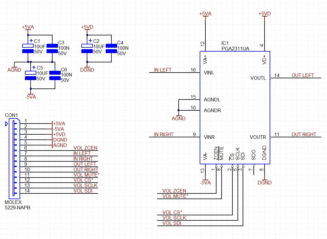
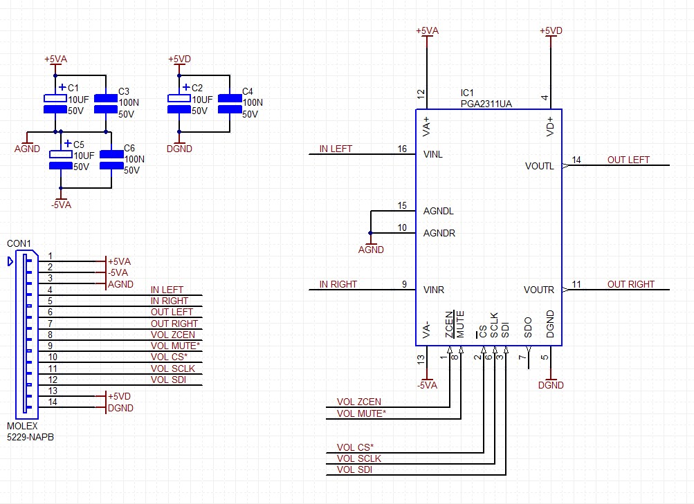
Consider the example schematic below. It is a simple volume control with analogue input and output signals, a digital control interface and a connector carrying all the signals, power and grounds required to make it work.
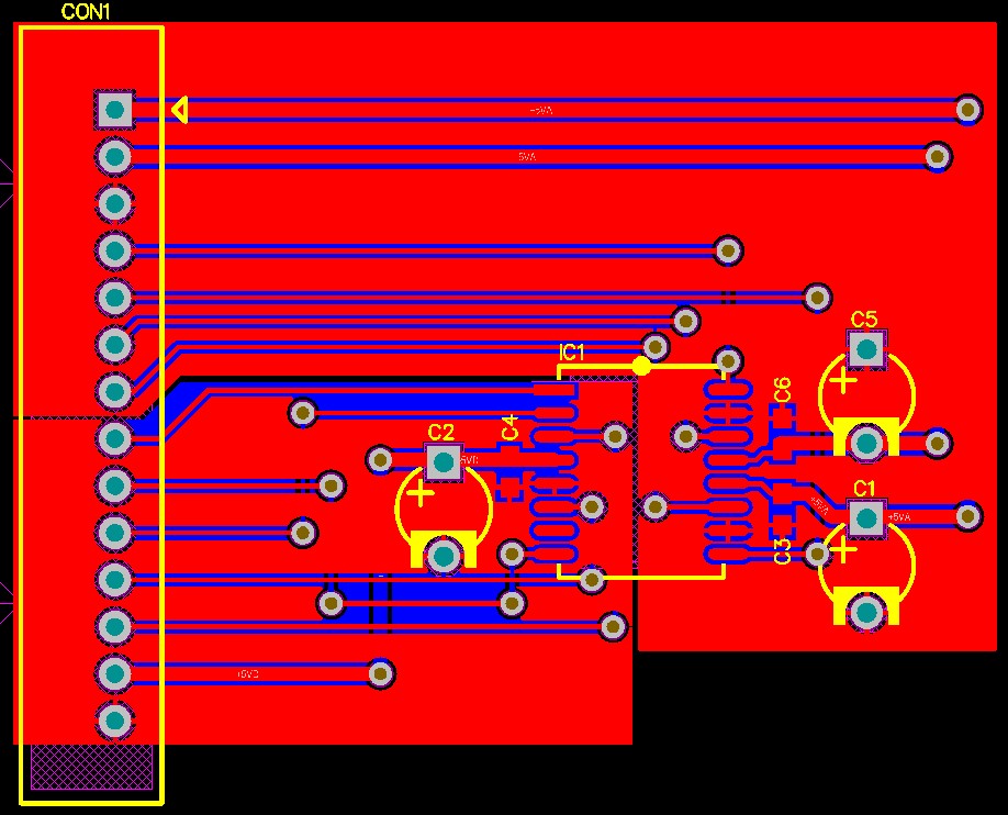
The design translated to the PCB layout software and the components arranged where we want them. We are now presented with what is generally known as the rats nest. This is where all the connections are shown simply as lines tracing the shortest distance between pins.
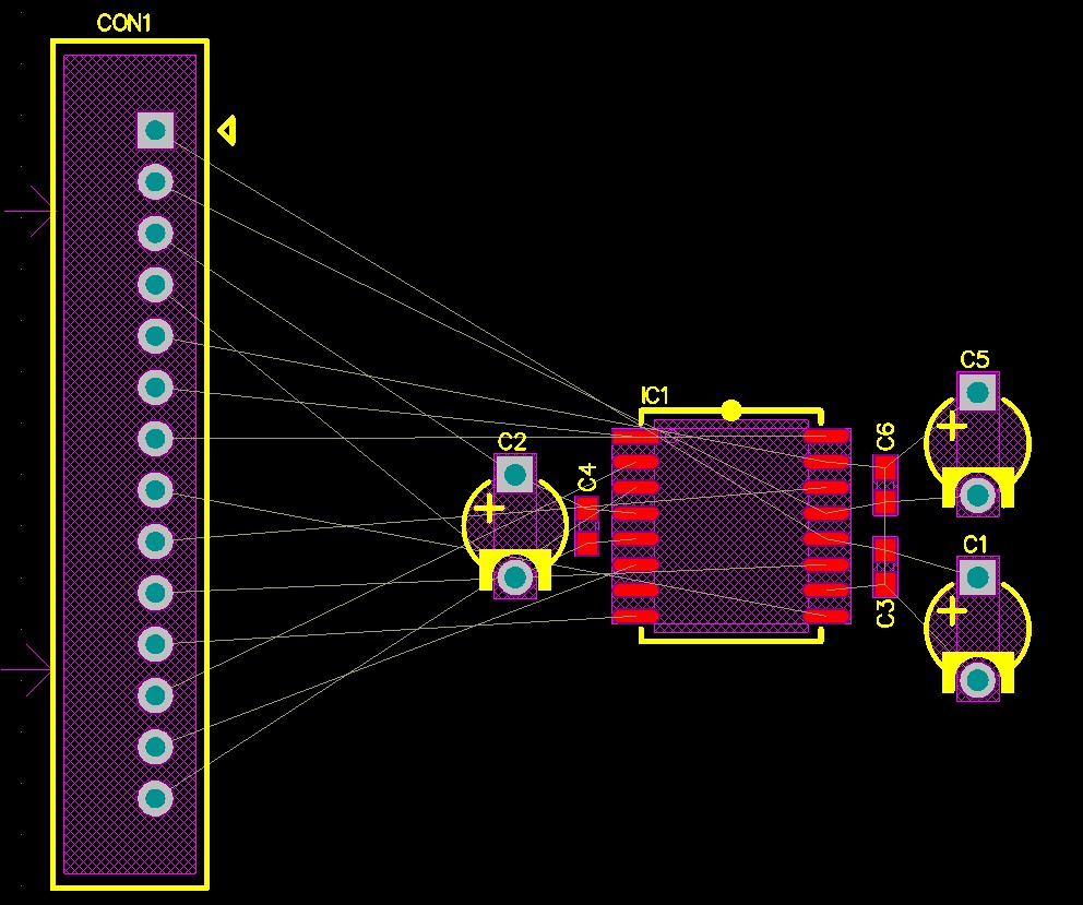
This is a very simple example with only a hand full of connections. A typical PCB will have hundreds of components with thousands of connections that need to be routed. As it is not possible to consider every connection of every component at the same time the easiest way to do this is to route each component or section of PCB then connect to the next component or section.
For the majority of signals they go from one component to another with no connections to any other components. In the case of power and ground connections these are typically connected to lots of components in different areas of the PCB. As these are arguably the most important connections, without them nothing will work at all, let alone well, it makes sense to route these first then deal with the rest of the rats nest of input and output signals.
So let’s route the power and ground... then route the rest of the connections:
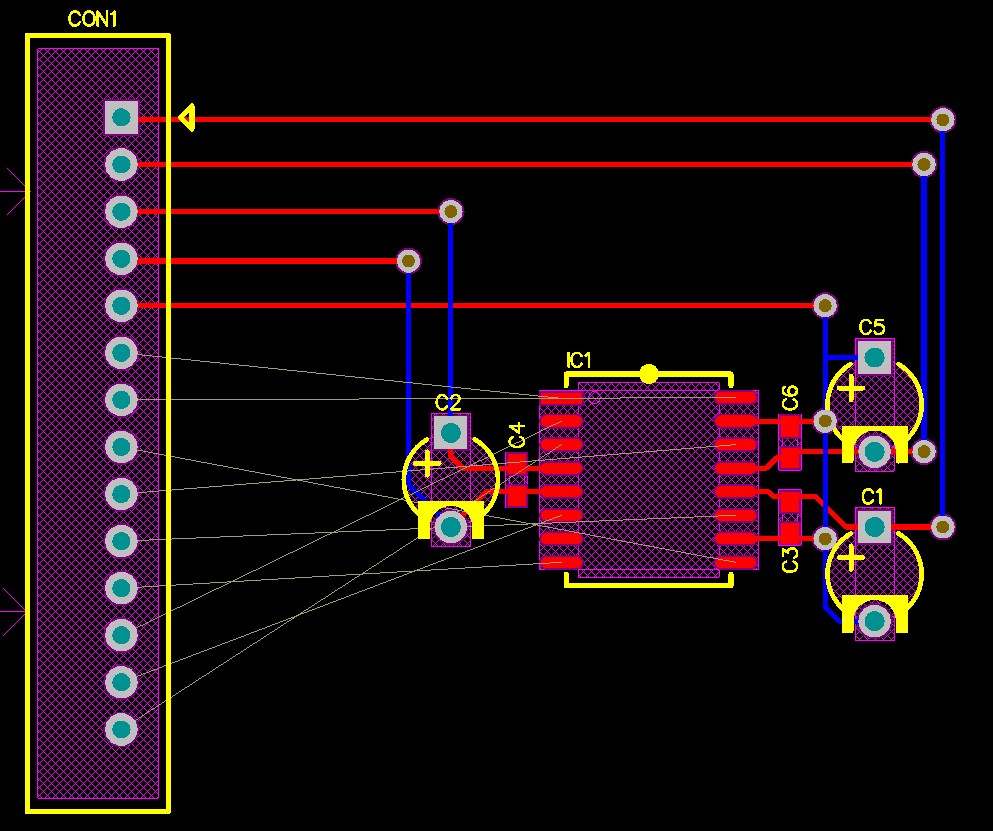
Suddenly looks a bit of a mess. It also has potential issues that may not come to light until you have the PCB made and start testing.
• There are high speed digital control signals very close to our analogue input and output signals which brings with it the potential for interference.
• There are long tracks for the power and ground pins which have an inherent resistance. In the case of this part it is not a big issue, but if this was a high speed part that was switching pins potentially millions of times a second the added resistance of these traces could cause the part to be starved of current and suddenly it cannot switch fast enough or at all. The result of which is the product stops working with no obvious reasons why.
• There is no easy path for the ground to return for the high speed signals or the analogue signals. The ground naturally wants to “follow” the input trace back to its source and this is not possible with this layout.
There are a number of approaches we could take to improve the layout, including:
1. Increase the width of the power and ground traces to lower their resistance.
2. Use a copper “flood” for the ground to lower its resistance and give the ground an easier route back to source whist being able to “follow” the input signal route.
3. Move parts and pins around to improve the routing.
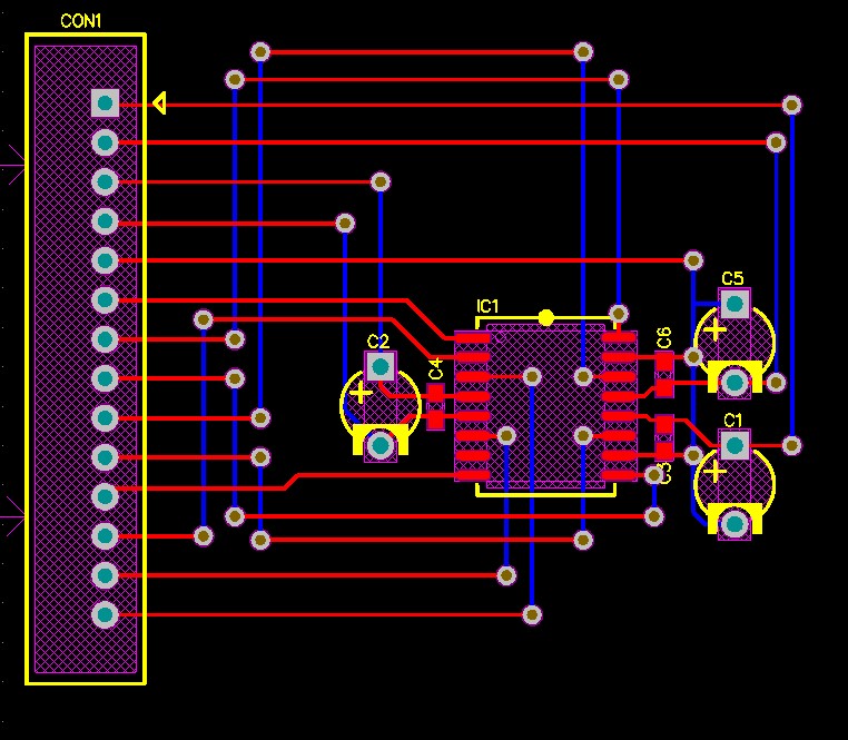
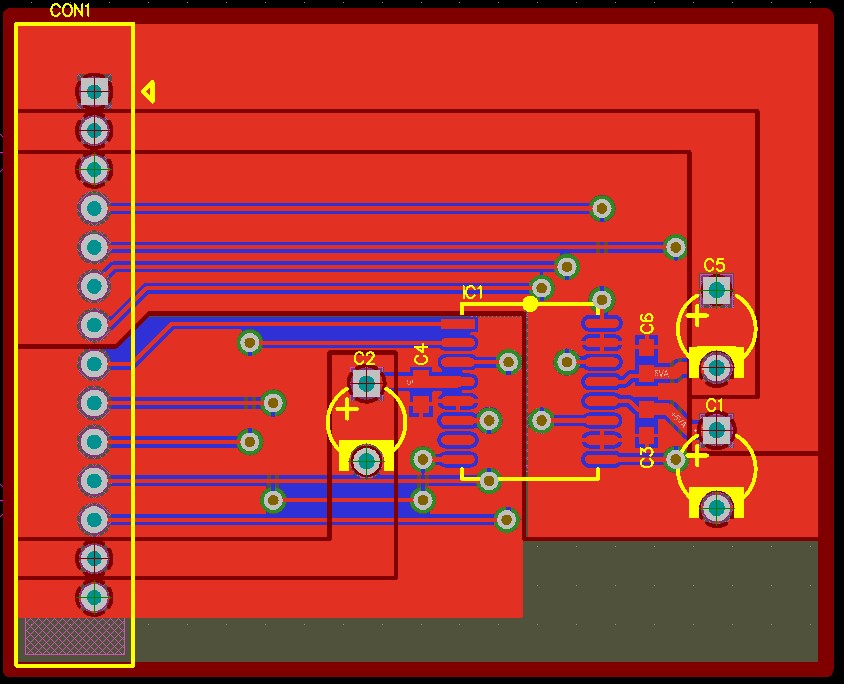
On the schematic the signals are reorganised so that the analogue power and ground are on pins adjacent to the analogue signals and the same for the digital control signals and power.
On the PCB the width of power traces is increased and the ground traces with copper floods. This results in the digital signals being surrounded by their associated ground and the same for the analogue signals.
This is a definite improvement from what we started with and hasn’t cost anything to do and uses no additonal parts or resources.
If we were routing a high speed component or one that requires mutiple different power rails we could consider using a multi layer PCB rather than the standard two layer type. This would enable us to use solid layers of copper on the inside of the PCB to carry our power and ground. This has the advantage of not having to route the power or ground as the copper layer takes care of it for us. It also means the lowest possible impedance for the power and ground due to the increased surface area of the power and ground regions.
So the final “ultimate” version of this simple example would look something like the graphic on the right.
Now we have addressed all the potential issues with best design practices and we can be confident that not only will the part work but it will also work as well as it possibly can.
For the purposes of this example this was all a bit overkill but when you are routing a real PCB then using multilayer PCBs, copper floods and putting some thought into your inter PCB and inter component connections will all make sure the design performs to the best of its ability. This is an iterative process that will probably take multiple tries in order to make sure all the critical signals and components are considered and taken care of. Something that is especially true when you are initially presented with the initial rats nest for a PCB for a real product. The picture below is what a real PCB for an integrated amplifier looks like with signals going all over the place.
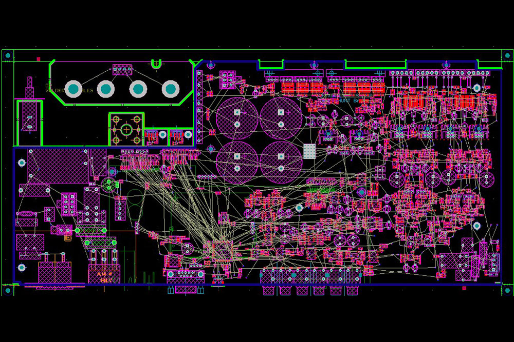
Being able to get all the power and ground routed and removed from the rats nest will then allow you to see the wood from the trees which will then allow you to concentrate on all the other critical signals in the design. There is nothing worse than spending hours routing the PCB only to find you now have no way to connect power to a component as you have filled up the PCB with all the other signals.
In summary, whilst you may have used the most expensive components in your design and you followed all the recommendations in the datasheet paying attention to the details could make the difference between a product that simply works, to one that is a class leader in its field.
Sometimes all it takes is a bit of copper that would have normally been etched away to make that difference.