Tech Talk
PCB Layout: How Good Practise Can Prevent Later Issues
By Jon Henderson
Hardware Design Engineer, Harman Luxury Audio

As a bright-eyed engineer, still filled with hope and looking to make my mark on the world, I would like to believe that a day is only wasted if you don’t learn anything new. As luck would have it, as the youngest member of my design team, there’s no shortage of learning opportunities that come my way on a daily basis. Unfortunately, some lessons are best learnt the hard way as I am about to explain.
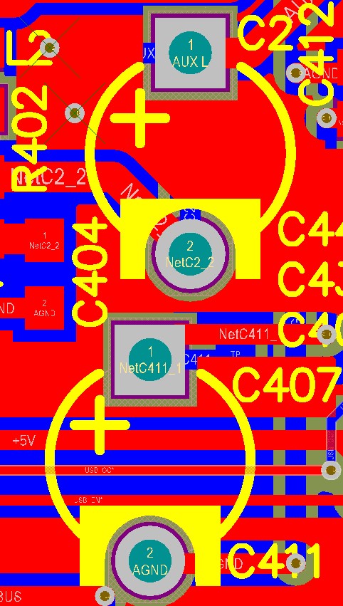
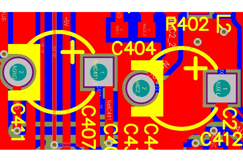
Figure 1
The Mistake
Consider Figure 1, which shows an image snipped from a recent PCB layout.
Here we see two electrolytic capacitors, one of which plays a vital role as part of the input to an ADC (Analogue to Digital Converter). In the interest of saving space, these two capacitors were placed closely together and at a first glance, there appears to be enough room for both of them. No errors have been flagged by the error-checker, so all good right?
Let’s take a look at Figure 2 and see what hidden details are revealed when I switch on the silk screen for the bottom layer.
In Figure 1, the bottom overlay was hidden so that the PCB appeared less cluttered when doing the layout. With the bottom overlay now enabled we can see two blue squares that have been squeezed together between the two capacitors. These squares indicate which way the pins will likely bend when the components are placed in the PCB, and as you can see they are slightly overlapping.
As always, hindsight is a wonderful thing and left unnoticed this PCB was released for a prototype build.
The Result
Jump forward a few weeks and these prototype boards are ready for some preliminary EMC (Electro-Magnetic Compliance) tests. The first test performed was to see what was radiating out the back of the unit, and the results were as follows (in Figure 3).
Figure 2
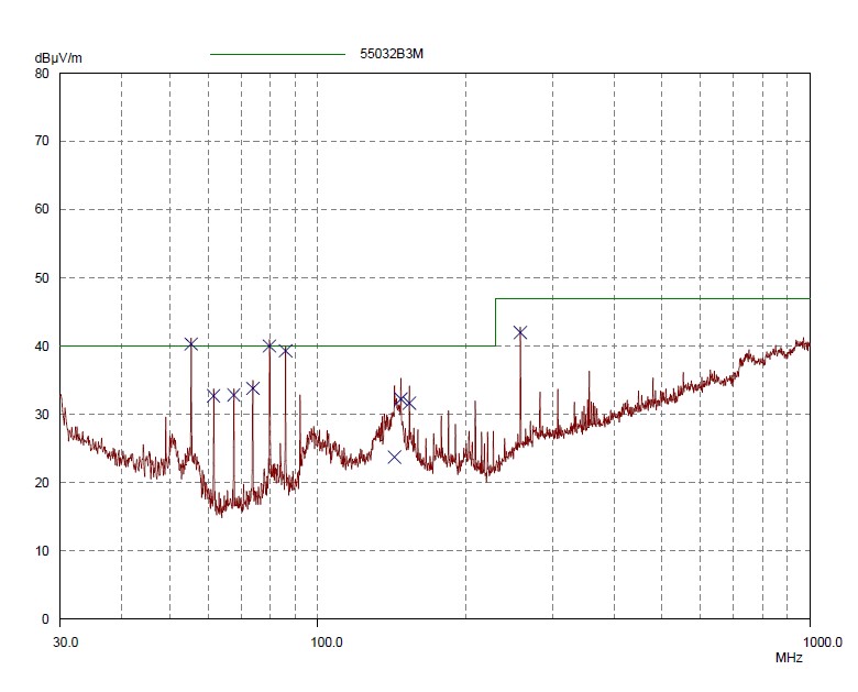
Figure 3: Radiated Emissions Results
Overall, this was not a bad result, but ultimately, a fail due to the unexpected spikes between 50MHz and 100MHz. This then led to a painfully frustrating day of fault-finding with little progress made.
One method of identifying which area of the unit is causing the failure, is to gradually unplug cables from the back and see how the measurements change. To my surprise, once the cable going to the analogue input was removed the spikes disappeared completely. This then prompted an investigation which led to the cause of the problem eventually being identified – The pins of the capacitors were shorted together.
The Moral of the Story
An easily overlooked mistake made early on in the development process can turn into a thorn in your side at a later date. Whilst error-checking tools are important for quickly identifying if any of the design rules have been broken, there is no substitute for good design practise and the knowledge gained from previous experiences.